Material Analysis with Invia Confocal Raman Microscope
The Invia Confocal Raman Microscope is an advanced tool used for material analysis based on Raman spectroscopy. This technology enables the identification of chemical structures, material stress, and molecular composition with high precision. Developed by Renishaw, this microscope is widely used in various fields such as pharmaceuticals, nanotechnology, material science, and biology.
Advantages of Invia Confocal Raman Microscope
• Non-Destructive Analysis with High Resolution
With a confocal system, this tool can focus laser light on a specific point of the sample, reducing interference from other layers. This makes it ideal for observing the internal structure of materials without the need for complex sample preparation.
• Advanced Optical System for Spectral Mapping
This microscope enables deep spectral mapping and provides quantitative information on the distribution of components within a sample. Features such as multiwavelength excitation and automated analysis capabilities further enhance research efficiency.
• LiveTrack™ Technology for Real-Time Scanning
One of the unique features of the Invia Confocal Raman Microscope is LiveTrack™, which allows real-time mapping of uneven surface samples without losing focus. This is particularly useful for analyzing materials with complex topographies.
(3D surface profile image of a metal coin demonstrating LiveTrack technology’s 3D optical microscopy ability. The coin’s dimensions were 18.0 mm diameter × 1.7 mm thick)
• High-Speed Imaging with StreamLine™ Technology
The StreamLine™ Imaging feature enables large-area mapping at high speed without compromising spectral resolution. With this technology, users can analyze samples in a shorter time while still obtaining accurate data.
StreamLine and LiveTrack technologies were used to image an ammonite fossil with a complex surface that is difficult to measure with other Raman systems. Variations in Raman bands from iron sulfide indicate areas of high compressive stress (red) and high tensile stress (blue)
• Highly Sensitive Detector with Automatic Filter Selection
This device is equipped with an automatic filter selection system and a highly sensitive detector, allowing it to detect very weak signals with high accuracy. This makes it an ideal solution for applications requiring a high level of sensitivity.
With its various advantages, the Invia Confocal Raman Microscope is the top choice for researchers and industries to gain deeper and more accurate insights into material properties.
Hysitron TI 980 TriboIndenter: A Breakthrough in Nanomechanical Testing
In the field of material research and development, precision and efficiency are crucial for accurately measuring mechanical properties at the nanoscale. Hysitron TI 980 TriboIndenter by Bruker stands out as an advanced solution, integrating cutting-edge technology to deliver speed, accuracy, and versatility in a single nanomechanical testing system.
One of its key innovations is NanoDMA® IIIwhich enables high-resolution dynamic viscoelastic analysis at a single sample point. Unlike traditional static methods, this feature provides superior accuracy, making it particularly beneficial for studying polymers, biomaterials, and composites.
Ceramic matrix composite modulus map composed of 400 measurements in 67 seconds
Additionally, XPM™ (Accelerated Property Mapping) revolutionizes property mapping by increasing measurement speed up to 100 times fasterthan conventional techniques. This allows for comprehensive material characterization over large areas in significantly less time. SPM+ (Scanning Probe Microscopy) the system offers high-resolution surface imaging, delivering deeper insights into material structures.
10 μm scan size, 1024 x 1024 resolution, topography image of a meteorite sample
Scan size and resolution of vertical and horizontal axes can be changed independently: 30 μm x 30 μm scan size, 256 x 256 resolution (top); and 60 μm x 30 μm scan size, 512 x 256 resolution (bottom)
To ensure measurement stability and precision Performech™ II Advanced Control Module provides ultra-precise force and displacement control with minimal noise. This guarantees consistent and highly accurate mechanical property evaluations, even for complex materials.
With its advanced technology, Hysitron TI 980 TriboIndenter is a powerful tool for a wide range of applications, including semiconductor research, thin film analysis, biomaterial characterization, and advanced structural materials. Its combination of speed, precision, and flexibility makes it the ideal choice for laboratories and industries that demand cutting-edge nanomechanical testing capabilities.
Basic Mechanical and Electrical Measurements for Li-ion and Solid-State Battery Materials Using AFM
Li-ion and solid-state batteries play a crucial role in the advancement of modern technology, from portable electronics to electric vehicles. The main challenge in the development of these batteries is improving efficiency, longevity, and safety, which requires an in-depth understanding of the electrode and electrolyte material properties at the nanoscale. Therefore, a characterization tool is needed that not only provides surface morphology data but also quantifies the mechanical and electrical properties of materials.
Atomic Force Microscopy (AFM) is essential in battery material research due to its ability to simultaneously detect mechanical, electrical, and morphological properties. Selecting the right AFM model is critical to obtaining accurate and relevant results in this field.
The Dimension Icon AFM from Bruker offers high-precision measurements, including the PeakForce QNM mode for analyzing mechanical properties such as elasticity modulus, adhesion strength, and deformation without damaging the surface. This mode is particularly useful for mapping mechanical changes in electrode layers due to repeated charging cycles and provides accurate quantitative data on complex surfaces. With the addition of the Conductive AFM (C-AFM) mode, this instrument enables electrical property analysis of materials at the nanoscale, making it a comprehensive solution for characterizing next-generation battery materials.
Carbon Nanotubes
Simultaneous topography and conductivity mapping of single-wall carbon nanotubes loosely attached to Au-patterned silicon using TR-TUNA, with 1 µm resolution.
For example, in battery material research such as carbon nanotubes (CNTs), AFM with TR-TUNA technique can map their conductivity at the nanoscale. This mapping provides valuable insights into the conductivity of CNTs and how their conductive properties interact with other material surfaces within battery components.
Material Science: Driving Innovation with Advanced Analytical Instruments
Innovation across industries, from flexible electronics to smart textiles, hinges on a deep understanding of material behavior at the nanoscale. The Anasys nanoIR3 revolutionizes material science by combining atomic force microscopy (AFM) with photothermal infrared spectroscopy, offering unmatched precision in high-resolution chemical analysis and nanoscale material characterization. At this microscopic level, materials reveal chemical and structural secrets that directly impact performance. For instance, the flexibility and strength of polymers, the seamless integration of composites, and the efficiency of semiconductors all depend on chemical composition mapping at the nanoscale.
Why is the Nanoscale Critical in Material Science?
The NanoIR3 empowers researchers to tackle critical challenges in material design. Its advanced capabilities allow precise visualization of polymer distributions, enabling the development of more durable materials for extreme conditions. In composites, it identifies weak spots, ensuring stronger and more reliable integration. For semiconductors, NanoIR3 uncovers the nanoscale structures that dictate energy efficiency and long-term stability, driving breakthroughs in electronics and solar cells.
nanoIR measurements on polymer nano fibers.
(John Rabolt et al, University of Delaware)
Pengukuran nanoIR pada Serat Nano Polimer (John Rabolt et al, Universitas Delaware)
Transforming Material Science with Anasys nanoIR3
The impact of this tool is far-reaching. It aids in crafting robust yet adaptable polymers for flexible electronics, mapping atomic distributions in superconductors for high-energy applications, and analyzing nanosensor integration in smart textiles to create garments that monitor health and performance. With its advanced biochemical imaging tools and unparalleled ability to perform nanoscale analysis, the Anasys nanoIR3 is not just an instrument—it is a catalyst for innovation, pushing the boundaries of material science and accelerating progress across industries.
Our use of plastics has skyrocketed, and now we’re finding these microplastics in everything from food chains to oceans. These little pieces don’t break down easily and might harm the environment, even ending up in us! To understand their impact, we need to identify them.
Raman spectroscopy: A powerful tool to see the small stuff
This technique lets us examine individual particles automatically and painlessly. Unlike other methods, Raman can analyze a wide range of particle sizes, from 1 micrometer to hundreds of micrometers. It can also tell similar materials apart very well. We can use Raman to study microplastics in anything from rivers to animal guts, even drinking water and the air!
Automating the analysis: Finding microplastics in bottled water
We filtered bottled water through a special filter and used a powerful microscope with Raman to analyze a tiny area. This area contained a lot of particles!
The image was analyzed using the Renishaw’s Particle Analysis module to produce a list of 5,663 particles for potential analysis. 3. In this case, the particles to target for analysis were chosen based on their size relative to the filter holes. The minimum particle area was limited to 4 µm2 (2.3 µm in diameter) producing 1,026 particles. The largest particle, fiber-like in aspect ratio, had a length of 147 µm. Each particle was analyzed sequentially and automatically using 532 nm laser excitation and a 50× objective. The microscope then automatically analyzed each particle, one by one.
What did we find?
We identified 18 different materials, including things like minerals, pigments, dyes, and of course, microplastics! We found that most of the particles were either polypropylene (a type of plastic) or calcium carbonate (a mineral). Smaller particles were mostly calcium carbonate, while larger ones were more likely to be polypropylene.
Raman can even identify dyes and pigments!
This information can help bottled water companies improve their filtration processes. Raman can even analyze particles with mixed components, like a particle containing both plastic and a pigment.
This powerful technique allows us to see and identify tiny plastic particles with incredible detail, helping us understand the microplastics problem.
Developing useful products with extremely thin films (less than 500nm) requires precise measurement of their mechanical properties. However, existing guidelines for testing these delicate layers become unreliable, especially for films thinner than 200nm.
The good news is that nanoindentation and nanoscratch testing offer a solution. These techniques allow direct and continuous measurement of critical properties like stiffness, strength, and wear resistance. They can even detect subtle damage in these ultra-thin films under various conditions (temperature, environment).
Nano technologies provide the necessary precision and control to measure these properties accurately, even for films just a few atomic layers thick. This allows researchers and engineers to develop reliable ultra-thin films for future products.
Based on foundational imaging techniques like Contact Mode and Tapping Mode, Bruker presents AFM methods that enable users to investigate the electrical, magnetic, or material characteristics of their samples. As scientific exploration advances, there's a growing need for a wider range of methods and approaches. Bruker's groundbreaking PeakForce Tapping technology introduces a fresh imaging approach integrated into various methods, delivering data on topography, electrical, and mechanical attributes concurrently.
Pushing the boundaries of data richness, the innovative DataCube Modes offer extensive hyperspectral data, including electrical transitions and force-distance profiles for each pixel. Additionally, AFM-nDMA evaluates the viscoelastic features along with their frequency-specific behaviors.
Sejak ditemukannya pada tahun 1991 oleh Sumio Ijima, carbon nanotube telah menarik perhatian peneliti. Hal ini disebabkan sifat elektoronik, termal, dan mekaniknya.
Seperti diketahui, carbon nanotube merupakan turunan struktur carbon yang dapat digambarkan sebagai lembaran grafit setebal 1 atom yang digulung menyerupai silinder dan berdiameter dengan order nanometer.
Carbon nanotube terbagi atas dua kelas berbeda, yakni Single Wall Carbon Nanotube (SWCNT) dan Multi Wall Carbon Nanotube (MWCNT). Pada SWCNT dinding nanotube hanya terdiri dari satu lapisan graphene saja.
Artinya, lembaran tersebut digulung tanpa celah untuk membentuk silinder berongga. Dengan demikian, kerap disebut sebagai nanotube graphene (GNTs).
Keunggulan SWCNT
Sifat unggul SWCNT dibandingkan multi-wall nanotube, yakni memiliki sifat listrik, termal, dan mekanik yang lebih baik. Bahkan, SWCNT memiliki kekuatan sepulu kali lebih kuat dibandingkan baja, dan enam kali lebih ringan. Contohnya, material komposit Single Wall Carbon Nanotube banyak dimanfaatkan di berbagai teknik, misalnya mengurangi bobot pesawat ruang angkasa sebesar 50%.
Lalu, SWCNT dapat menunjukkan karakteristik listrik logam atau semikonduktor berdasarkan diameter dan kiralitasnya sehingga cocok untuk nanoscale wires dan komponen listrik. Sementara itu, konduktivitas termalnya yang tinggi menjadikannya sebagai materials yang tepat untuk sensor jarak maupun aplikasi lainnya.
Analisis Single Wall Carbon Nanotube dengan Raman
Meskipun Single Wall Carbon Nanotube memiliki berbagai keunggulan sayangnya, ia berukuran kecil dan memiliki kepadatan tinggi. Karena itu, menjadikannya sulit untuk dikarakterisasi dengan metode tradisional.
Salah satu, metode analisis yang dapat mengkarakterisasi Single Wall Carbon Nanotube dengan tepat, yaitu Raman Spectroscopy. Metode Raman Spectroscopy merupakan salah satu teknik analisis utama untuk mengkarakterisasi SWCNT.
Spektrum Raman sendiri, digunakan untuk menentukan diameter tabung, kiralitas, sifat elektronik, dan regangan yang terdapat baik dalam sampel nanotube massal dan tersisolasi.
Structural and Chemical Analyser (SCA) dari Renishaw adalah sistem yang menggabungkan Raman microscopy dengan Scanning Electron Microscope (SEM). Tentunya, hal ini menjadikan penentuan lokasi dan analisis Raman SWCNTs terisolasi dapat dilakukan dengan cepat dan mudah.
SCA bekerja dengan menggunakan SEM untuk memvisualisasikan permukaan sampel. Nantinya, Raman spectrometer berguna untuk mengumpulkan spektrum dari area tertentu pada gambar. Dengan demikian, proses identifikasi dan penentuan lokasi SWCNTs dapat dilakukan tanpa perlu memindahkan sampel atau optik pengumpulan.
SCA digunakan untuk mempelajari sampel massal SWCNTs. Spektra Raman menunjukkan bahwa sampel tersebut mengandung Single Wall Carbon Nanotube dengan diameter berkisar 0,9 – 1,3 nanometer.
SCA juga dapat digunakan untuk mempelajari sampel mikro SWCNTs yang diorientasikan di antara dua gold electrodes. Spektra Raman menunjukkan bahwa nanotube dalam sampel mikro memiliki diameter yang sama, yakni 1,1 nanometet.
Tidak hanya itu, SCA telah digunakan untuk mempelajari single nanotube yang disuspensi dalam cairan. Spektra Raman menunjukkan bahwa SWCNT bersifat logam.
Keunggulan Structural and Chemical Analyser (SCA) Renishaw
SCA adalah instrumen serbaguna yang dapat digunakan dari Renishaw untuk mempelajari berbagai sampel Single Wall Carbon Nanotube dengan cepat dan akurat. Berikut manfaat SCA dalam penentuan lokasi dan analisis Raman dengan cepat dari SWNTs terisolasi.
SCA menggabungkan kekuatan pemisahan dan visualisasi SEM dengan kekuatan identifikasi kimia dan fisik spektroskopi Raman.
SCA dapat digunakan untuk menentukan lokasi sampel dengan SEM dan mengkarakterisasi sifat kimia dan strukturalnya dengan Raman, tanpa harus memindahkan sampel atau optik.
SCA, instrumen serbaguna yang dapat digunakan untuk mempelajari berbagai sampel SWNT.
SCA instrumen yang cepat dan akurat, menjadikannya alat yang ideal untuk aplikasi penelitian.
Tribolab adalah sebuah tribometer skala laboratorium yang diproduksi oleh Bruker. Biasanya, tribolab dapat digunakan untuk menguji berbagai jenis surfaces, termasuk logam, plastik, dan keramik.
Pengembangan lubricants dan surfaces pada mesin reciprocating dan kompresor kian dilakukan. Karenanya, pengukuran kinerja lubricants menjadi faktor kritis dalam estimasi akurat efisiensi bahan bakar.
Sebab itu, dalam melakukan hal tersebut diperlukannya tribometer skala laboratorium. Evaluasi tribologi pada sistem reciprocating dapat dilakukan secara efektif pada skala laboratorium melalui penerapan profil gerakan dan kecepatan yang tepat sehingga dapat mensimulasikan gerakan sebenarnya dari tribosistem.
Sistem reciprocating dalam sistem tribologi
Saat melakukan sistem reciprocating diperlukanya pemilihan elemen yang berperan penting dalam sistem tribologi, seperti di bawah ini.
Material dan geometri sampel yang diuji
Tekanan kontak antara permukaan yang dikendalikan oleh beban, geometri, dan material permukaan kontak
Frekuensi reciprocating dan panjang stroke yang akan mengarahkan profil gerakan dan kecepatan
Suhu terkendali nantinya mengaktivasi peristiwa tribo-kimia pada permukaan yang diuji
Tidak hanya itu, dibutuhkan pula beberapa faktor parameter utama yang diukur selama pengujian. Berikut parameter utama yang dimaksud.
Perubahan gesekan sepanjang stroke, karena gesekan tidak stabil dalam sistem recprocating
Perubahan suhu
Keausan yang diukur setelah pengujian.
Keunggulan penggunaan tribometer
Penggunaan tribometer skala kecil memiliki keuntungan tersendiri, yakni lubricants dan surfaces dapat dengan mudah dikarakterisasi setelah pengujian dengan menggunakan alat meterologi lainnya, seperti profilometer dan analisis kimia/spektrometer.
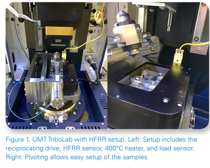
Di bawah ini, terdapat gambar 1 yang menunjukkan setup TriboLab untuk pengujian reciprocating dengan frekuensi tinggi. Setup ini dilengkapi tahap fast reciprocating stage, piezo-based sensor, normal-force sensor, dan pemanas 400°C.
Rakitan sensor telah dirancang dengan kemampuan berputar agar pengguna dapat mengganti sampel yang lebih rendah dengan cepat dan mengaplikasikan lubricants.
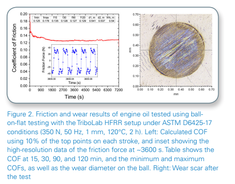
Gambar 2 menunjukkan hasil dari pengujian engine oil 5W-30 menggunakan konfigurasi reciprocating ball-on-flat (steel-on-steel) dan sistem ASTM D6425-17 dengan setup HFRR. Selanjutnya, perubahan gesekan diamati dan diplot sebagai fungsi waktu, data dikumpulkan dan direkam dalam resolusi tinggi untuk memantau variasi kecil gesekan sepanjang stroke.
Variasi gesekan sepanjang stroke umumnya disebabkan oleh kombinasi perubahan pada permukaan, peralihan pada lubricants, dan getaran yang dihasilkan dari gerakan mekanis. Dari data resolusi tinggi ini, perubahan arah mudah divisualisasikan.
Berikutnya, gambar 3 menunjukkan koefisien gesekan (COF) sebagai fungsi posisi. Hal ini dikarenakan kecepatannya termasuk sinusoidal bukan linear.
Pun, terdapat sistem HFRR sehingga dapat melakukan pencatatan posisi yang tepat sebab menggunakan LVDT (transformator perpindahan variabel linier) yang terintegrasi dalam tahap reciprocating cepat. Grafik ini, dengan jelas menunjukkan bagaimana gesekan mencapai maksimum di setiap titik ekstrik stroke serta bagaimana perubahan arah berikutnya.
UMT Tribolab Bruker
Software pendukung pada UMT Tribolab Bruker memberikan fleksibelitas penuh kepada pengguna untuk menganalisis data yang diperoleh dari pengujian reciprocating dengan frekuensi tinggi.
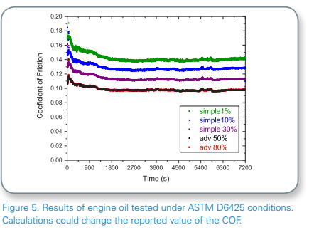
Lalu, dalam menghitung COF pengguna dapat memilih dari beberapa metode, seperti metode sederhana yang menggunakan persentase nilai gesekan tertinggi di tiap stroke (Gambar 4 kiri) atau metode advanced yang memilih persentase titik di tengah stroke (Gambar 4 kanan).
Tentunya, kemampuan ini membantu user dalam menyesuaikan pengumpulan dan analisis data kemudian, memberikan nilai gesekan yang dapat membantu memahami perbedaan kecil antar lubricants.
Pada gambar 5 menunjukkan perbedaan antara perhitungan COF secara keseluruhan saat menggunakan metode yang berbeda untuk engine oil yang sama.
Saat menghitung COF dengan metode yang berbeda, dapat dilihat bagaimana nilai COF berubah secara dramatis dari nilai keseluruhan sekitar ~0,14 saat menggunakan metode sederhana dengan 1% dari top point menjadi ~0,11.
Selanjutnya, saat menggunakan 30% dari top point menjadi lebih rendah (~0,10). Pun, saat menggunakan metode advanced dengan 50% dari titik di tengah stroke. Metode advanced cenderung lebih konsisten dengan 50% dan 80% dari overlapping points.
Dengan demikian metode sederhana kurang konsisten dibandingkan metode advanced. Akan tetapi, metode ini tetap diperlukan untuk menghitung gesekan dari puncak ke puncak (persentase kecil dari top points) sesuai dengan standar ASTM.
Begitupun, metode yang dipilih untuk menghitung COF sangat penting dalam melakukan perbandingan lubricants yang paling dekat dengan performance. Hal ini tidak hanya nilai absolut sederhana saat mengacu pada gesekan sistem reciprocating, namun sangat bergantung pada metode analisis.
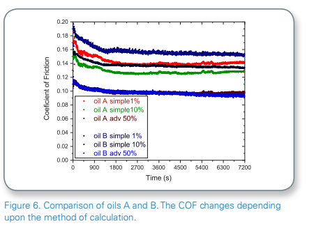
Dalam gambar 6 menerangkan bahwa pengujian yang dilakukan dengan ASTM D6425-17 pada dua lubricants (oil A:5W-30, oil B:0W-20) yang mendekati performancenya dan bagaimana data dapat berbeda dalam metode yang digunakan.
Saat menggunakan metode sederhana dengan 1% dari top points, perbedaan antara oils A dan B dapat lebih terlihat. Hal ini sangat berbeda jika dibandingkan saat menggunakan metode advanced dengan 50% dari points yang mana kondisi lubricants overlapping.
Rig reciprocating frekuensi tinggi dari UMT Tribolab terbukti sebagai teknik yang dapat diandalkan untuk skrining material dan pelumas pada aplikasi recprocating, misalnya mesin dan kompresor.
Fleksibelitas sistem ini, menjadikan evaluasi lubricants pada sistem yang berbeda serta dengan keunggulan untuk mengendalikan analisis data. Bahkan, UMT Tribolab dapat melakukan protokol serupa dengan ASTM 6425 untuk mengevaluasi gesekan pada lubricants serta membantu perbedaan penting dalam berbagai fungsi tribosistem.
Molekul biologis pertama yang dividualisasikan oleh Atomic Force Microscopy (AFM) ialah DNA. Hal ini dilakukan untuk mempelajari struktur, topologi, dinamika DNA, dan bagaimana interaksinya dengan protein. Teknologi PeakForce Tapping Mode ekslusif dari Bruker dapat melakukan imaging double helix DNA dengan resolusi tinggi yang dapat mengukur kekuatan imaging tanpa memerlukan probe khusus ataupun design AFM yang terbatas.
Pengenalan AFM ke dalam penelitian Biologi
Pada awal tahun 90-an pengenalan TappingMode meningkat secara signifikan dalam penggunaan AFM untuk penelitian biologi. Dalam TappingMode, probe berosilasi pada frekuensi resonansi fundamental dengan posisi vertikal dari tip (atau sampel) kemudian disesuaikan untuk mempertahankan amplitude osilasi yang konstan saat probe melakukan scan melewati surface.
Sayangnya, Tapping Mode menghasilkan resolusi gambar lebih rendah dibandingkan Contact Mode AFM. Untuk itu, faktor utama dalam meraih hasil gambar AFM berkualitas tinggi membutuhkan kontrol gaya interaksi antara probe dan sampel selama proses imaging.
Tahun 2010, Bruker memperkenalkan PeakForce Tapping Mode dalam AFM. Metode yang digunakan secara luas dalam penelitian biomolekuler sebab kemampuannya menghasilkan gambar beresolusi tinggi secara konsisten.
Pada PeakForce Tapping, jarak antara probe dan sampel dimodulasi secara sinusoidal dengan mempertahankan gaya maksimum antara keduanya.
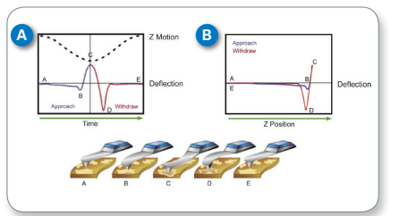
Gambar 1. In PeakForce Tapping Mode the AFM probe is modulated at low frequency (1-2 kHz). (A) As the probe is brought into contact with the surface, the feedback signal is the maximum or “peak” force applied to the surface. (B) If the motion of the probe is considered in terms of Z position, one is essentially performing a force curve at every position of the sample surface
Feedback loop waktu secara nyata digunakan untuk mengontrol posisi probe dan penggunaan sinusoidal ramping sehingga kecepatan scanning lebih tinggi. Bahkan, teknologi PeakForce Tapping menggunakaan mode imaging ScanAsyst yang mengoptimalisasi setpoint imaging secara otomatis.
Metode PeakForce Tapping Mode pada DNA
Metode PeakForce Tapping Mode berhasil melakukan imaging DNA dengan resolusi tinggi. Hingga saat ini, DNA merupakan contoh sampel yang tepat untuk teknik tersebut serta telah banyak diimaging menggunakan AFM.
Pada gambar DNA, struktur heliks ganda dapat terlihat dengan jelas. Dalam beberapa penelitian sebelumnya, DNA diadsorpsi pada permukaan mika kemudian dimodifikasi untuk menciptakan interface positif. Hadirnya kontrol gaya interaksi antara probe dan DNA mengakibatkan proses imaging DNA dalam kondisi fisiologis yang lebih relevan.
Gambar 2. PeakForce Tapping image of groove depth variations in the DNA plasmid topography obtained using the FastScan Bio AFM and FastScan-D probes (small cantilever and standard silicon tip). (A) Low-magnification AFM topography image of a plasmid showing corrugation. The white rectangle indicates the area imaged in B. (B) Higher-magnification trace (white arrow to right) and retrace (white arrow to left) images of this area showing corrugation consistent with the B form of DNA, for consecutive images. (C) Trace (solid) and retrace (dashed) height profiles taken along straight lines as indicated in B, closely following the backbone of the four plasmid scans and averaged over a 5 -pixel (~0.5) width. The height profiles confirm the observed corrugation to be the alternating major and minor grooves of double helix structure and that these grooves vary in depth along the DNA strand. The height profiles have been offset by multiples of 0.6 nm for clarity. Color scales: 3.5 nm (A), 1.1 nm (B). Reproduced with permission from Pyne et al.3
Beberapa keuntungan yang dimiliki imaging DNA melalui metode PeakForce Tapping Mode, yakni melindungi probe dan sampel dari kerusakan potensial dengan menggunakan gaya imaging rendah. Tidak hanya itu, metode ini dapat memudahkan proses imaging fluida lingkungan.
Tentunya, hal ini berbeda dengan metode Tapping Mode yang mana tidak ada kebutuhan untuk mengatur kantilever dan pengoptimalan otomatis dalam metode ScanAsyst meningkatkan kecepatan dan konsistensi imaging.